

Nanoseminar
Group of Structure analysis at the Department of Condensed Matter Physics
of Charles University and MGML has a pleasure to invite you to attend the seminar on nanomaterials: Physics, Technology, Applications
on 16th April 2026 at 14:00
at Faculty of Mathematics and Physics of Charles University, Ke Karlovu 5, 121 16 Praha 2
Lecture room F2
Miroslav Šlouf
4D-STEM-in-SEM: Walking through Dimensions
Miroslav Šlouf » 4D-STEM-in-SEM: Walking through Dimensions
Location: F2
4D-STEM-in-SEM: Walking through Dimensions
Miroslav Šlouf1, Pavlína Síkorová2, Ewa Pavlová1, Vladislav Kryzanek2
1 Institute of Macromolecular Chemistry, Czech Academy of Sciences, Praha, Czech Republic
2 Institute of Scientific Instruments, Czech Academy of Sciences, Brno, Czech Republic
The advent of 2D array detectors of transmitted electrons (pixelated detectors) have revolutionized the field of electron microscopy. A microscope equipped with a pixelated detector scans an ultrathin specimen, recording the position of the electron beam on the specimen (X, Y) together with positions of all scattered electrons on the detector (x, y). If the scanning beam is quasi-parallel, the individual images (x, y) are nanobeam diffraction patterns (NBD). The resulting scanning transmission electron microscopy (STEM) dataset is four dimensional (X, Y, x, y) and the method is called 4D-STEM [1].
Fig.1
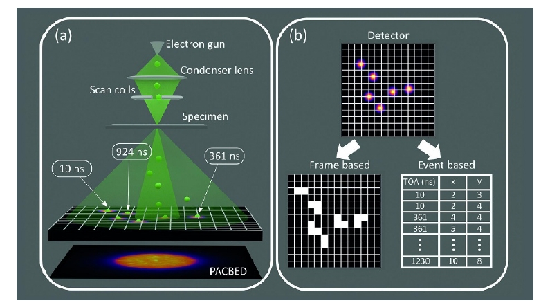
Fig. 1. Frame-based and event-based detectors for 4D-STEM. The frame-based readout consists in the collection of 2D-array of 2D-NBD patterns. The event-based readout produces a 1D stream of data packets, where each packet corresponds to a single event – when electron strikes the detector chip [2].
In our project, we have developed three open-source Python packages for 4D-STEM-in-SEM.The first package (Reader4D; [3]) reads/visualizes/checks 4D-STEM data. The second (STEMDIFF; [4]) reduces 4D-STEM datasets to 2D powder diffraction patterns. The third (EDIFF; [5]) converts the experimental 2D-diffractograms to radially averaged 1D-profiles (ELD) and compares them with the theoretical powder X-ray diffraction patterns of the expected crystal structure (XRD). All three packages are focused on user-friendliness and automation, so that they could be used by common SEM users without deep crystallographic background.
In this contribution, we will explain how we reduce 4D datasets to 2D patterns and final 1D profiles, which is a basis of our new technique called 4D-STEM-PNBD [6]. We will discuss the specific processing of datasets from frame-based detectors (4D-STEM as 2D array of 2D-NBDs) and event-based detector (4D-STEM as 1D stream of events). Finally, we will outline the future development of our software packages (monocrystal patterns, more automation, AI tools etc.).
[1] Ophus C (2019): Microscopy and Microanalysis. DOI: 10.1017/S1431927619000497.
[2] https://analyticalscience.wiley.com/content/article-do/4d-stem-event-based-electron-detection
[3] https://github.com/pavlinasik/Reader4D
[4] https://pypi.org/project/stemdiff (and references therein)
[5] https://pypi.org/project/ediff (and references therein)
[6] Slouf M (2025): Microscopy and Microanalysis. DOI: 10.1093/mam/ozaf045
e-mail: slouf@imc.cas.cz

If you wish to receive regular updates on fothcoming seminars, contact M. Dopita.
