

Seminar on Structure Analysis
Group of Structure analysis at the Department of Condensed Matter Physics
of Charles University and MGML has a pleasure to invite you to attend the seminar
on 17th May 2023 at 13:10
at Faculty of Mathematics and Physics of Charles University, Ke Karlovu 5, 121 16 Praha 2
Seminar room F 052
Anna Macková
Nuclear Physics Institute of the Czech Academy of Sciences, Řež
Key role of ion beam technologies for application in microelectronics, optics and sensors
Anna Macková » Key role of ion beam technologies for application in microelectronics, optics and sensors
Nuclear Physics Institute of the Czech Academy of Sciences, Řež
Location: KFKL seminar room, F052
KEY ROLE OF ION BEAM TECHNOLOGIES FOR APPLICATION IN MICROELECTRONICS, OPTICS AND SENSORS
A. Mackováa,b*, A. Jagerováa,b, P. Malinsky´a,b, M. Cutroneoa, P. Nekvindovác, A. Michalcovád, V. Holýe, Z. Soferc, S. Akhmadalievd, R. Böttgerd
aNuclear Physics Institute of the Czech Academy of Sciences, v. v. i., 250 68 Řež, Czech Republic
bDepartment of Physics, Faculty of Science, J.E. Purkinje University, Česke Mládeže 8, 400 96 Ústí nad Labem, Czech Republic
cDepartment of Inorganic Chemistry, University of Chemistry and Technology, 166 28 Prague, Czech Republic
dDepartment of Metals and Corrosion Engineering, University of Chemistry and Technology, 166 28 Prague, Czech Republic
eDepartment of Condensed Matter Physics, Faculty of Mathematics and Physics, Charles University Ke Karlovu 5, 121 16 Prague 2, Czech Republic
dInstitute of Ion Beam Physics and Materials Research, Helmholtz Zentrum Dresden-Rossendorf, 01328, Dresden, Germany
Due to its versatility, the ion beam technology is an attractive and commonly used method for the incorporation of various ions into a single- and nano-crystal ZnO structure, bulk ZnO nanostructuring, optical active particle/defects engineering, surface nano-pattering and lithography. The latter one is nowadays important as well in semiconductors as in graphene oxide. Both so distinct materials find their application in sensing and bionics applications with the functionalization via ion beam technology. Metal oxides based efficient photocatalysts can be an efficient green approach for relieving the negative environmental influence of organic pollutants on the ecosystem [1,2]. Noble metal nanoparticles can expand the light absorption range of ZnO and can greatly enhance the ZnO photocatalytic activity given their plasmonic or luminescence properties [3, 4], a use of enriched ZnO nanostructures as nanosized biosensors has also been explored for the detection of different biological molecules [5]. Defect clustering and engineering, dopant interaction with defects in ZnO after ion implantation/irradiation allow formation of doped-nanocrystallites to be controlled and tuned in ZnO.
Graphene-like materials have aroused significant interest for supercapacitors and ultrasensitive gas detectors because of their remarkably high carrier mobility, extraordinary surface area, 2D structure and cost-effective easy-to-prepare nanoscale morphologies [6]. Graphene oxide (GO) is decorated with epoxides and hydroxyls on basal planes and carbonyls and carboxyls on the edges, which increase the hydrophilicity of GO and consequently enhance its sensitivity to water molecules [6]. Ion lithography can be successfully used for microscale device preparation in GO prospective for flexible electronics as well as for sensing applications see Fig. 1 [6, 7]. The microscale capacitors in GO can respond to external stimuli, such as voltage, mechanical deformation, temperature, light and electrochemical reduction/oxidation processes [8]. In both above mentioned materials the ion beam technology has been successfully used for nano and microstructuring, optical response tuning and surface nano-patterning/lithography enabling new prospective applications [3, 8, 9, 10].
Acknowledgement
The research has been carried out at the CANAM (Centre of Accelerators and Nuclear Analytical Methods) infrastructure. This research was supported by the projects GACR No. 19-02482S and No. 22-10536S.
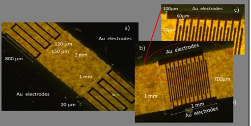
Optical microscope images of the GO microcapacitor examples prepared by the C-ion, 5MeV via ion beam lithography.
References:
- J.Liu, Y.Wang, J.Ma, Y.Peng, A.Wan, Journal of Alloys and Compounds 783 (2019) 898.
- M.Samadi, M.Zirak, A.Naseri, E.Khorashadizade, A.Z.Moshfegh, Thin Solid Films 605 (2016) 2.
- 3. Macková, P. Malinský, A. Jagerová et al, Vacuum 169 (2019) 108892.
- L.Ma, S.Chen, Y.Shao, Y.L.Chen, M.X.Liu, H.X.Li, T.L.Mao, S.J.Ding, Catalysts 8 (2018) 634.
- E.Danielson, V.Dhamodharan, A. Porkovich, P. Kumar et al, Sci. Rep. 9 (2019) 17370.
- D. Zhang, J. Tong, B. Xia, Q. Xue, Sensor Actuat B-Chem. 203 (2014) 263–270.
- A. Lamberti, F. Perrucci, M. Caprioli, M. Serrapede, M. Fontana, S. Bianco, S. Ferrero, E. Tresso, Nanotechnology 28 (2017) 174002.
- P. Malinský, A. Romanenko, A. Macková et al, Applied Surface Science 528 (2020) 146802.
- P. Nekvindová, J. Cajzl, A. Macková, et al, Journal of Alloys and Compounds 816 (2020) 152455.
- A.Macková, A.Jagerová, P.Malinsky, M.Cutroneo, J.Flaks, P.Nekvindová, A.Michalcová, V.Holý, T.Košutová, Physical Chemistry Chemical Physics 22(41) (2020) 23563-23573.
- A.Yu Azarov, E.Wendler, A.Yu Kuznetsov, B.G. Svensson, Appl. Phys. Lett. 104 (2014) 052101.
- A.Yu Azarov, A.Hallén, X.L.Du, P.Rauwel, A.Yu Kuznetsov, B.G. Svensson, J. Appl. Phys. 115 (7) (2014) 073512.
- B. Jany, N. Gauquelin, T. Willhammar, M. Nikiel, K. H. W. van den Bos, et al, Sci. Rep. 7 (2017) 42420.

If you wish to receive regular updates on fothcoming seminars, contact M. Dopita.
